Agilent 101: An Introduction to Nanotechnology
|
|
Nanotechnology scientists work with structures that are less than 100 nanometers in at least one dimension. To understand the scales that nanotechnology encompasses, the images below show the sizes of well-known structures. The width of a human hair is about 70 microns (10-6 meters). Cells are on the order of one micron. DNA is a few nanometers (10-9meters) wide. Atoms are a few angstroms (one angstrom equals one tenth of a nanometer) in scale. Human hair grows at a rate of about 4 nanometers per second.
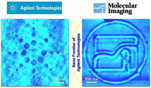
The images below were created after Agilent acquired atomic force microscope (AFM) company Molecular Imaging in 2005. The image on the left shows the Agilent “spark of innovation” logo. Inside the smallest “spark” on the right-hand side of the image is the Molecular Imaging logo. The image was created with an AFM, which was used to etch the two logos into a standard computer CD and then image the two logos. To put the scale in perspective, the Agilent logo is about 70 microns across – about the size of a human hair.
Nanotechnology markets and customers There are three broad market classifications for nanotechnology customers: materials, biology and semiconductor. Materials customers account for about 50 percent of the business, and biology and semiconductor customers split the rest of the market. Customers are working on problems as diverse as fabricating next-generation semiconductors, manipulating cells to detect cancer, finding the best way to remove gum (a polymer) from sidewalks, making tires last longer, making LCD screens that don’t scratch in your pocket, and making razor blades that don’t last too long. Agilent’s measurement customers in nanotechnology want to do three things: image, characterize and manipulate structures at the nanometer scale. Imaging is easy to understand: Scientists often need a visual representation of structures. Optical microscopes don’t work below a few hundred nanometers because that is the scale of the wavelength of light. The two most commonly used techniques for imaging below the optical limit are scanning electron microscopes and atomic force microscopes. Characterization can take the form of electrical, mechanical and chemical characterization. Customers want to understand these properties on small structures and how they change with nano-scale spatial resolutions. For example, semiconductor engineers may want to understand how dielectric properties change across a wafer. Biologists may want to understand how the mechanical stiffness of cancer cells differs from healthy cells. Material scientists may want to understand the location and chemical properties of contaminants in structures. Manipulation is being able to move molecules or atoms to affect the properties of a structure, such as a cell or a semiconductor. Nanotechnology measurement customers are primarily researchers. Approximately 80 percent of our customers are in academia or government laboratories. The remaining 20 percent are in industry. Academic customers in the United States typically rely on government agencies such as the National Science Foundation, the National Institutes of Health, the Department of Energy and the Department of Defense for funding. Most countries and the European Union have similar organizations that fund academic research. Our customers are generally professors who run large research programs. They are called primary investigators, and these PIs generally have teams that include post-doctoral students, doctoral students and laboratory technicians. They buy tools for specific purposes or projects, or for use as shared equipment by multiple PIs or across entire institutions. Most customers have doctorates in biology, material science, physics or chemistry. Agilent’s nanotechnology solutions Agilent's Nanotechnology Measurements Operation (NMO) offers a variety of nanotechnology solutions in three categories.
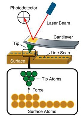
Atomic force microscopy produces true three-dimensional images. Much in the way an old-fashioned record player’s needle moved across the surface of a record and “read” the information in the grooves, an AFM reads the height of a cantilever that has a sharp tip on the end. The AFM scans the surface in the X and Y direction, taking a Z height measurement at each pixel on the image. The Z height is measured by bouncing a laser off the back of the cantilever so it hits a split photo detector. As the cantilever moves up and down in the Z direction – while it is scanned across the surface – the amount of light hitting the top and bottom halves of the detector determines the Z height. AFM imaging is a relatively slow technique, with images of 512 x 512 pixels taking a few minutes to obtain. AFMs are relatively slow because the tip is touching the surface, but the fact that it touches the sample allows multiple measurements at the same time. For example, topography and current can be measured simultaneously. Agilent has a unique solution that attaches a PNA network analyzer to the AFM to make an S11 (return loss) measurement while obtaining a topography image. This allows for the creation of a spatial map of complex impedance with tens-of-nanometers resolution. Another advantage of AFMs is that samples do not need to be coated or dried to take an image. AFMs can work in many different environments, including liquids, high humidity, and hot and cold temperatures. This allows scientists to image samples in preferred environments. For example, an AFM can image a live cell in a liquid bath, which is needed to keep the cell alive. An AFM system consists of a:
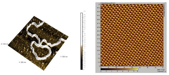
Below are images taken on an AFM. The first image is of DNA. The second is of graphite. On the graphite sample, each bump represents a carbon atom, which is 2.4 angstroms – or 0.24 nanometer – in size.
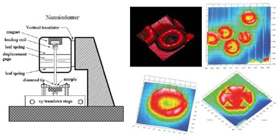
The second measurement technique, nanoindentation, gives researchers key insights into a wide variety of physical characteristics of materials under test. Nanoindentation is used to measure hardness; elastic and plastic compliance of surfaces; and tribological properties such as wear resistance, adhesion, fracture toughness, thin-film homogeneity and creep. Nanoindenters are similar to AFMs in that the instruments touch the surface of samples with a sharp tip. However, nanoindenters press on the surface with a force that is perpendicular to the surface. The instrument is used to push into, or indent, the surface. While the indentation is occurring, the controller measures the force the indenter is exerting on the sample and the distance the tip has moved into the surface of the sample. This creates a “force distance curve,” which can be used to calculate the modulus of the sample.
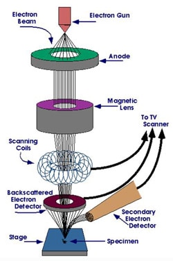
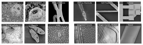
NMO’s newest business, scanning electron microscopy (SEM), is the most popular method of obtaining images of structures that are too small to be seen on optical microscopes. Instead of using light to create the images, electrons are used as the illumination source. Electrons have a much smaller wavelength than light, and therefore allow for imaging of structures in the single-digit nanometer range. The diagram below shows the basic structure of a scanning electron microscope. It consists of:
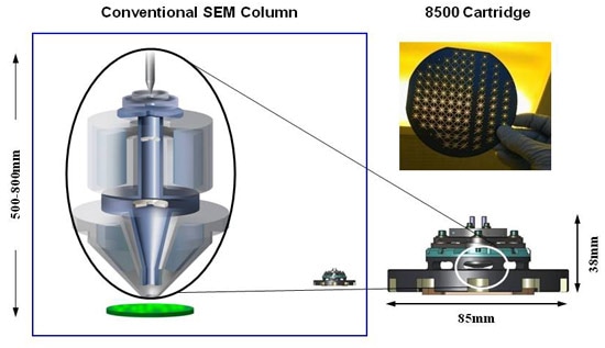
An image is created pixel by pixel as the beam is scanned across the surface. Most SEMs use electromagnetic lenses for focusing the beam. The lenses are large, often need to be water-cooled, and suffer from hysteresis (the lagging of an effect behind its cause). Agilent’s key innovation is a lens that is electrostatic instead of electromagnetic. This allows the column to be much smaller, avoiding the need for water-cooling and eliminating hysteresis. The slide below shows the size advantage of the Agilent electrostatic column.
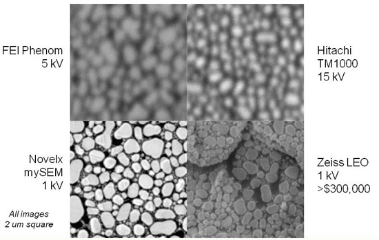
High-resolution SEMs capable of nanometer resolutions range in price from $300,000 to more than $1 million. About five years ago, major players in the SEM market introduced tabletop SEMs. These systems sold for less than $100,000, did not need special facilities such as cooled water or three-phase power, and fit on a tabletop. However, they exhibit relatively poor performance – on the order of 40-nanometer resolution. The Agilent system is compact – about the size of a LaserJet printer – and does not need special facilities, but has resolution specifications close to systems costing $300,000 or more. Agilent has priced the 8500 SEM between the high-resolution systems and the low-performance tabletop systems. The image below shows how the 8500 stacks up against high-end and tabletop systems.
Nanotechnology as a growth initiative Nanotechnology remains one of the most promising growth initiatives for Agilent and EMG. Members of Agilent’s executive leadership team, including EMG President Ron Nersesian, have considered long-term technology and industry trends as well as competitive moves and concluded that we must be a leading provider of nanotechnology solutions. That means Agilent will continue to invest in NMO to maximize our competitiveness.
|