Frontiers of Electronic Measurement
|
|
October 16, 2009“Measurement is a cornerstone of scientific progress, at the heart of many of the most important and challenging problems in technology and society today,” says Darlene Solomon, Agilent’s chief technology officer. For 70 years, Hewlett-Packard Company and Agilent Technologies have contributed technologies and developed solutions for test and measurement customers. Much of that innovation is currently driven out of the company’s central research laboratories.
“Measurement has enabled the development of exciting new technologies and products that are integral to our lives,” Darlene says. She points to the example of cell phones. Today, cell phones are pervasive – ‘must-haves’ right up there with food, shelter and water – in both developed and developing societies. Evolving mobile technologies continue to blur the lines between our physical and virtual worlds. “Back in the early 1970s, who could have envisioned what this mobile device would do today?” Darlene asks. “Even more, what do we see for the future in other technologies, as we push beyond today’s traditional spaces?” Darlene highlights three areas that represent current frontiers of electronic measurement. Non-linear measurements For more than 40 years, scattering parameters – also known as “S-parameters” – have been among the most important foundations of microwave theory and techniques. S-parameters revolutionized the world’s ability to measure, model and design linear components. By knowing the measurements of the S-parameters of a device, it is possible to completely characterize the device’s linear behavior. Over the past 40 years, HP and Agilent have developed an entire line of vector network analyzers that measure linear parameters, enabling huge advances in the design of small-signal components and systems. Today, however, efficiency requirements are driving active devices to behave in nonlinear ways.
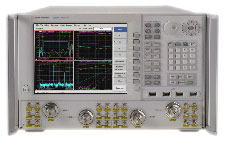
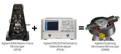
Agilent: X-parameters Much work has been done across the industry trying to develop other parameters to characterize nonlinear behavior. However, these other parameters – such as TOI, P1dB, ACPR and EVM – only roughly describe nonlinear behavior. In addition, they require several different instruments. Agilent has developed X-parameters, the scientific superset of S-parameters. “X-parameters can do everything that S-parameters do for linear components and systems,” says Darlene. “In addition, they encompass key nonlinear properties that S-parameters can’t handle.” Agilent’s nonlinear vector network analyzer is the first and only instrument on the market that can measure X-parameters. Time-synchronized measurement Another challenge for customers is that increasingly complex measurement and control problems require coordinated, integrated data acquisition and signal generation. There is an increasing need for multiple instruments to work together. As Agilent’s Measurement Research Laboratory began researching this topic, one of the biggest challenges was how to coordinate joint actions between two or more different instruments. In our daily lives, we coordinate actions and events based on time for meetings, plane flights, etc. It is routine for us to use calendars and clocks to coordinate joint activity, but instruments haven’t been able to do this. Agilent has developed and collaborated with standards bodies to enable synchronized clocks inside instruments. Measurements from participating instruments can now be time stamped, which is a significant step forward in correlating measurement results across instruments. Measurements and signals can be initiated by “time triggers,” which complement traditional hard-wired trigger methodologies. An example can be found in the airplane testing industry. A typical airframe design certification test may require more than 3,000 sensors to measure stresses, strains and pressures to determine airworthiness. The problem has been traditionally solved by running separate analog cables from every sensor back to a single instrument. Once collected, the measurement data is passed to a computer for further analysis. However, this solution is far from ideal. In addition to the large expense, the long analog cable runs are susceptible to noise that may degrade the measurements significantly. Agilent: LXI and IEEE 1588 standards Agilent’s modular instruments are designed around LXI (LAN eXtensions for Instruments), a standard led by Agilent and a consortium of companies. The LXI standard defines small, modular instruments using low-cost, open-standard LAN (Ethernet) as the system backbone. A key part of LXI is the IEEE 1588 time synchronization standard that Agilent Labs invented and helped standardize. Today, IEEE 1588 is finding wide use across a number of different industries that require very precise time accuracy, and time-sync features are required in LXI Class-B instruments. “With 1588, all instruments are time synchronized with each other and produce measurements with accurate timestamps and time triggers,” Darlene says. “Multiple instruments can work together, each one measuring a subset of the channels.” For example, in flight test using LXI/1588 across distributed instruments, analog cable runs can be minimized while measurement accuracy improves. All of the data flows back to the computer via simple network cables for further analysis. Building accurate distributed measurement systems for situations such as flight test design are now feasible. Nanotechnology Historically, physics, chemistry, biology and electronics have been discrete disciplines. Each has relied upon its own measurement systems, with very little overlap. Today there is much more overlap, and nanotechnology is one major factor driving this convergence. “Today,” says Darlene, “we are on the cusp of being able to understand, manipulate and measure devices, systems and living things on the molecular or nano scale.” The majority of research investment in nanotechnology today is in electronic and information technology. This is being driven by increasing demands for miniaturization and integration, as the industry strives to keep pace with Moore’s Law. (Moore’s Law predicts that electronics performance will continue to double every two years.) However, most experts agree that the greatest potential impact of nanotechnology will be in health care and life sciences. Nanotechnology could enable new classes of therapeutics and therapeutic delivery that can be targeted at the cellular and molecular levels, new biomaterials for synthetic or artificial skin, and many other mind-boggling possibilities. According to Darlene, “technology convergence will drive the need for exciting new measurements.” With expertise in both electronic and bio-analytical measurement, Agilent is uniquely positioned to emerge as a leader in measurement convergence at the nanoscale. Agilent: Microscopy At the end of last year, Agilent introduced an entirely new measurement platform: the Scanning Microwave Microscope (SMM). This new platform combined two existing Agilent products: the Vector Network Analyzer, which probes electronic properties; and the Atomic Force Microscope (AFM), which measures surface topology. “This is a nice example of the kind of synergy that is possible through Agilent’s unique breadth of measurement capabilities,” says Darlene. The SMM platform is the world’s first commercial scanning multi-frequency, absolute capacitance AFM. The combination of world-class microwave electronics with world-class AFM results in applications that were never before possible.
“Looking forward, we believe there will be many other applications where SMM provides unique and compelling value,” says Darlene, “including organic films, multilayer coatings and biological samples.” Darlene is excited as Agilent continues its research into the frontiers of measurement. “Measurement is all around us,” she says, “and Agilent’s singular focus is to provide leading measurement solutions to make this world a better place to live.” |